
Optomec, a manufacturer of industrial 3D printers, has received a set of new patents covering the use of its气溶胶喷气机3D printing technologyfor the production of 3D micro-structures.
该过程通常用于印刷电子应用,可以用分辨率降低到仅15微米的零件制造零件。这实际上是人类的眼睛看不见的,大约是人头发的宽度。Optomec展示了其令人印象深刻的气溶胶射流功能,具有多种材料类型,包括聚合物,复合材料,甚至金属。
With the issuing of the new patents, the company’s IP portfolio now totals more 75 patents, and includes global protection across the US, Asia, and Europe.
Dr. Michael Renn, CTO of Optomec, has been attributed with the new patents, bringing his personal tally to more than 50. He states, “Optomec continues to invest heavily in its core technology, seeking to extend the already broad range of applications for its Aerosol Jet solution. The capability demonstrated with our 3D Printed Micro-structures work is already seeing potential applications in Semiconductor Packaging and Medical Device markets.”
How does Aerosol Jet work?
气溶胶喷射3D打印作品通过精确地将少量电子油墨沉积到基板上。可抛弃的墨水首先放在雾化器中,在该雾化器中创建了浓密的墨水液滴。每个液滴的直径在1至5微米之间。然后将墨水从喷嘴中喷射出鞘胶,该喷嘴可用戒指包围气雾剂墨水。Optomec系统通常将干氮或压缩空气用作鞘气。
当气体和墨水穿过喷嘴的尖端时,它们会加速,而3D打印气溶胶材料将自己聚焦于紧密的液滴中。同时,鞘气可以与任何材料接触中的喷嘴绝缘,因此堵塞绝不是问题。
由于油墨用于气溶胶喷射可以对施暴者ed with conductive silver nanoparticles, the 3D printing technique lends itself quite well to electronics applications. This includes components such as resistors, capacitors, antennas, sensors, and thin film transistors – all of which have been fabricated on Optomec systems in the past. The performances of these components can also be closely controlled via the printing parameters of the Aerosol Jet 3D printer.

Scaling down to the micron
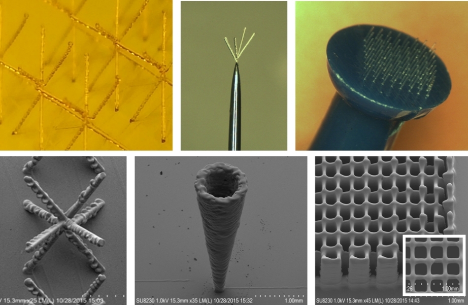
Optomec’s new patents, including美国专利号10,994473,通过利用原位加热或紫外线照明来描述3D打印微结构的方法,以在沉积时修改气溶胶油墨的机械性能。
In the case of UV illumination, the light would partially cure the photopolymer ink droplets in-flight, while a heating element would cause solvent-based inks to rapidly dry via evaporation. According to the document, this has the effect of increasing the aerosol ink’s viscosity, enabling it to form miniscule, free-standing 3D structures. This technique has allowed Optomec to achieve lateral resolutions of 15 microns, along with layer thicknesses of 100 nanometers and aspect ratios of 100x for millimeter-tall structures.
Still, Aerosol Jet isn’t the only additive manufacturing technology capable of microstructure fabrication. Earlier this year, scientists from the弗莱堡大学used two-photon-polymerization (2PP) technology from 3D printer manufacturerNanoscribeto fabricate glass silica microstructures with aresolution of just a few tenths of a micrometer。Using the company’s novel ‘Glassomer’ polymer-based resin, the team 3D printed objects with a surface roughness of 6 nanometers, much less than the 40-200 nanometers seen in many other glass parts.
在其他地方,3D打印机OEMNanofabrica还为自己建立了一个名字flagship Tera 250 microprinting system。TERA 250在Micro-DLP灯发动机上运行,并通过将紫外线投射到充满聚合物树脂的增值税中,并将其一层固化成3D构建。该系统能够在相对较大的构建体积上实现令人印象深刻的单微晶分辨率,尺寸为50 x 50 x 100mm。
Subscribe to the3D打印行业newsletterfor the latest news in additive manufacturing. You can also stay connected by following us on推特, liking us onFacebook,然后调查3D打印行业YouTube频道。
Looking for a career in additive manufacturing? Visit3D打印作业在行业中选择一系列角色。
特色图显示了通过气溶胶射流打印的微观结构3D。通过Optomec图像。