
I spoke with Simon Fried, CBO and Co-Founder ofNano Dimension, about 3D printing electronics, nano-technology and how to raise money for 3D printing ventures.
Founded in 2012, the Israeli company has a remarkable long-term vision for 3D printing. “Our vision is in 10 years from now we’ll have 3D printers that are 10 meters long, printing 6 or 7 different materials and possibly including assembly along the way,” says Fried. “We see our DragonFly 2020 printer and materials as a first footstep on the way to genuinely opening the doors to factories in a box.”
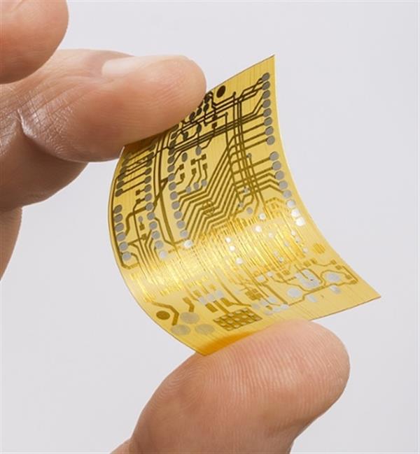
In the near term the company is focused on the release of its Dragonfly 2020, a piezo-inkjet based 3D printer designed to print electronics using multiple materials. Nano Dimension have developed propriety 3D printing technology and materials they say will enable rapid-prototyping of multilayer printed circuit boards (PCBs). The Dragonfly 2020 was demoed at this years CES and prompted a wave of media coverage that the company has ridden since, I ask Fried to clear up a few of the rumors and he is happy to oblige.
The first rumor is about the selling price of the Dragonfly 2020; reports have frequently speculated the 3D printer will come with a price tag in the region of $50,000. This is not to be the case. “The system is nearer to a couple of hundred [thousand] rather than fifty,” says Fried. He points to the fact that this is the price range where other enterprise level 3D printers from Stratasys and 3D Systems are. “I like to say well it’s about the same price but you can print in 2 materials and you’re getting different materials to boot,” adds Fried.
The second rumor is about the launch date of the Dragonfly 2020. Fried is confident that sales will begin by the end of 2016. He says customers will be, “Companies that we’re talking with today already,” and “the wider commercial distribution will be a story for 2017 and will evolve as the year unfolds.” Fried also puts to bed speculation about the materials that will be available on launch saying, “The immediate core ink that goes with the silver will be a rigidFR4-esque dielectric material.”
您如何3D打印电子产品?
One method to 3D print electronics is the Aerosol Jet system developed byOptomecand used in the manufacture of smartphones by their clients. Another manufacturer, Voltera, raised just over $500k on Kickstarter and began shipping to backers earlier in July. Voltera’s V-One 3D printer was initially based on inkjet printing but the company switched to swappable print heads and cartridges filled with more viscous inks in early 2014. As a reward for their support “early bird” customers were able purchase the 3D printer for $1199. The regular pre-order price is $2,199 for the printer, $99 for conductive ink cartridges and $49 for solder paste cartridges.
Voxel8 are currently selling their extrusion-based printer for $8,999, it uses PLA and also silver ink that costs $75. The Voxel8 prints with separate heads to deposit the thermoplastic and conductive ink, but these are both mounted on a single carriage so the need to swap out mid-print is removed.
Nano Dimension’s Dragonfly 2020 uses piezo inkjet type deposition to 3D print electronics. “You have one print head per material and you have lots and lots of nozzles per head, so its not the piezo dispensing which you see with solder paste sometimes, but its wide format industrial piezo heads,” says Fried.
Piezoelectric materials expand, and also contract, in response to voltage. When such materials are placed in a confined space with a liquid material, like ink, this property can be used to squeeze the liquid through a nozzle. “The end result is basically a board which if you pick it up it looks a little like a block of epoxy where the conductor traces are suspended within the block,” says Fried.
这说起来容易做起来难,因为Dragonfly 2020与两种截然不同的材料(导电墨水和聚合物绝缘子或介电材料)一起使用。Fried解释说:“您可以固化聚合物,并且您对纳米颗粒墨水进行烧结,而诀窍是要有一种材料的过程,而不是无意中损害其他材料的过程。”关键在于等离子波。
A Plasmon is not quite a particle; technically it’s a quasiparticle and related to the elusive Higgs-Boson. Nano Dimension harness this emergent phenomena whereby the nanoparticles in their inks absorb optical energy and create a plasmonic wave, a sort of electron surf. As the surf breaks the plasmonic wave changes state, and releases heat. It is the heat that activates the insulating ink and cures it. So, while the silver metal nanoparticles are sintered the insulating dielectric is cured and hardens. Plasmonic waves may have applications in nano imprint lithography to make the next generation of semi-conductors or tocure cancer by selectively targeting only abnormal cells.

A 3D printing world-first?
“我们不知道任何甚至可以作为最终用途的产品朝这个方向推动的事情,当然不是在专业水平上。”弗里德说。“专业的电子材料,受控的阻抗,高电导率,回流焊料并与行业集成,而不是用可用的产品来竭尽所能。”如果纳米尺寸在那儿提供的话,对PCB和3D打印景观的调查会支持他。“我们可以舒适地打印多层板,我们正在打印您在PCB中期望的所有功能。”他继续说:“目前它的8层,所有支持的功能,并追踪到125微米的痕迹和空间是我们在可靠的标签下所做的事情。”
但是,”the end goal is 3.5 mil, 90 micron trace and space, and anything up to a thickness of 3 millimeters, which is maybe one design’s 16 layer or another design’s 20 plus layer.” Currently 3D printed electronics are in the 250+ micron range for Voltera and Voxel8, althoughOptomec’s Aerosol Jet can go down to 10 microns. But it is the promised multi-layer capability enabled by the Nano Dimensions inks that have generated much of the buzz.
Fried tells me, “The world of conductive inks is now quite a big one.” Over the past year the conductive inks market has seen a, “real uptick.” He adds, “also the readiness and understanding of the relevant companies to really start looking for real applications rather than just a passing interest in the technology.”
“It’s the next big thing, and has been for some time, this time it looks to be for real” he says. Nano Dimension reviewed other inks on the market and found them lacking. Fried says, “They weren’t delivering the kind of conductivity that we needed for signal and power, as opposed to just signal.” The company is currently running its printers, “24/7” as part of in house testing and at some point over the next 10 weeks they will install the first systems offsite. If the feedback is positive it would not be a surprise to hear more news after that point.
An unusual approach to financing
“是有原因的,他们称它为硬件,哈尔d,” said Tony Fadell who brought Apple’s iPod to market. Anyone who has dipped a foot in the start-up waters whether via Kickstarter or at a grander scale will appreciate this. Although by no means an easy ride,software focused start-ups are often looked on more favorably by early stage investorssuch as angels or venture capitalists (VCs). This is because scaling software has far fewer real world tangible barriers.
“I don’t think any particular route to that funding nirvana is an easy one,” says Fried. But the company’s chosen funding vehicle seems particularly arduous and relatively unusual. Nano Dimension became listed on the NASDAQ as an ADR in March this year under the ticker NNDM, but its initial public listing was in Tel Aviv. In 2014, the company raised $1.5 million through a reverse merger on the Tel Aviv Stock Exchange (TASE). This is in essence; in effect the takeover of a public listed shelf company.
根据Tase的说法,自2014年以来,该国仅进行了11次反向合并,这是一种不寻常的融资方法,因此我要求Fried解释该决定背后的理由。
“It wasn’t the first startup for any of the founders and the usual route of angels or VCs proved to be very, very difficult because the amount of the capital required to get it off the ground,” Fried tells me. This was because of, “advanced hardware, but also quite tricky software and the cherry on top is the chemistry,” he says. The triple threat of software, hardware and chemistry were, “too big of a bite for any angels and too risky for the VC’s. We had them with the software, we got them a bit nervous with the hardware and then the slam-dunk was ‘oh by the way, there’s a ton of nano-chemistry as well’.”
With VCs, “running for the exit saying ‘great idea, love it, good luck,’” Nano Dimension did find a group of private investors willing to fund the company who, “insisted on it been a listed entity” as a, “liquidity get out clause,” says Fried. The golden lining is that, “I think follow on rounds have proven to be easier [and] balanced more towards the interests of the company,” he says.
With $7.5m in cash and equivalents on the balance sheet using the $1.2m Q1 spend as indicative of future requirements, the company will either need to book sales before March 2017 or access additional capital.
“Hardware is difficult to fund, and this as a complex multidisciplinary system is even more challenging to get initial funding for,” sums up Fried.
The silicon valley of inkjet
With HP Indigo, Stratasys, Scitex, Scodix, Xjet and others Israel’s tech industry seems to have an obsession with inkjet printing. Fried says, “There is a real cluster around the Rehovot Science Park where we are based.” This has advantages, theeconomic benefits of tech clusters弗里德说,有充分的文献记载,也创造了一个“经历了一个或两个周期的人的健康生态系统,将产品送出了门。”但是,集群并非没有问题,因此可能会出现如此多的技术问题。
距离纳米尺寸的道路约一公里,XJET也正在制造3D打印机,也使用nanoparticle metal inkjetting technology. Hanan Gothait is the co-founder of Objet and when his company was acquired by Stratasys he left to join Xjet where he is now CEO. Linked In lists five current employees of Nano Dimension who previously worked at Xjet, two more than those with Stratasys on their CVs. In a lawsuit filed in March 2015 Xjet, “has alleged that one or more of our [Nano Dimension] officers and/or employees previously employed by XJet stole trade secrets and proprietary technology relating to inkjet printing and 3D printing,” according to documents filed with the SEC as part of Nano Dimension’s listing on the NASDAQ.
XJET从Nano Dimension中寻求约520万美元的损失,更令人担忧的是,要求,如果成功的情况下,更糟的是,可以防止出售2020年蜻蜓2020,并以最小的延迟推出。纳米维度坚定地否认了指控。弗里德说:“当然,这是一条现场电线,但我们充满信心,我们会被免除。”我问何时可能会裁定此案:“它正在通过法院努力,法院将做法院将要做的事情,陪审团实际上是在这一问题上。”
When approached for this article, a spokesperson for Xjet said, “The lawsuit we filed against Nano Dimension and others is pending in court and being resolved through legal means. Beyond that, we do not want to respond on this matter.” Whatever the merits of the case, this is not the first time, nor will it be last, a tech company has been involved in litigation over intellectual property. Only those with intimate knowledge of the case may know the full truth.
地平线
The next six months will be an interesting time for Nano Dimension. As the company embarks on external testing, seeks to refine its printer and software and scales up production of conductive inks. “At the moment we make them in lab quantities, using a lab type facility and over the next 6 months we’ll be building out a volume production capability,” says Fried. Once the Dragonfly 2020 is out in the wild the market will undoubtedly cast its judgment on the pre-launch claims. Resolution of the lawsuit may yet determine when that launch takes place.
Nano Dimension has a growing intellectual property portfolio including an approach to 3D printed biotech. The combination of 3D printing and biotechnology can already producefunctional human tissuesand in the future may allow organs to be printed.
Nano Dimension最近宣布与Accellta建立合作伙伴关系,Accellta是一家使用3D悬架生物反应器培养和区分人类干细胞的公司。尽管可行性研究是成功的,并且可行的干细胞已成功印刷,但“我们的生物技术活动非常在燃烧器上,但胚胎是描述它的方式,我们不会让这些活动干扰我们的核心业务,”弗里德说。
西蒙·弗里德(Simon Fried)乐观,已经展望未来。他说:“我们可能会谈论很多关于PCB的知识,但是有很多东西可以利用我们的材料,并且知道人们最终将如何使用我们的系统。”鉴于这种多物质3D打印技术的潜力以及右手的创新纳米喷墨技术的可能性令人着迷。
Fried suggests, “It would be interesting to have one in for example in a place like the [MIT] Media Lab and to come back a year later.” As 3D printing makes further advancements into the electrical engineering space the next generation of printers will enable some remarkable applications. Perhaps, Nano Dimension 3D printers might well be one of the tools behind such future innovations.