
German electronics 3D printing specialistInnovationLab已经提出了一种制造印刷电路板(PCB)的低成本,更环保的方式。
作为一部分开发‘SmartEEs2’ EU Horizon 2020 project,该过程可以生产可遗传的铜电路,同时使用的能量比传统方法少,并避免了对有毒蚀刻剂的需求。现在据说该公司与合作伙伴Isra一起使用该技术,据说该公司开发了原型PCB,这可以作为新一代灵活,可穿戴电子产品的基础。
“This is a state-of-the-art production process, which will decrease costs and reduce logistical dependencies on suppliers while consuming fewer materials, using less energy and producing less waste,” said Dr. Janusz Schinke, Head of Printed Electronics at InnovationLab. “By the end of this year, we expect to have scaled this process to high volumes, meeting customer demands of a million solderable tracks or more.”
InnovationLab’s PCB R&D drive
InnovationLab is a self-proclaimed ‘one-stop shop’ for printed electronics, with a network of industry and academic partners, via which it’s able to support customers’ R&D efforts. Alongside this offering, the firm has established a portfolio of flexible printed pressure sensors, including itsBaMoS EV battery monitor和伴随Sensormatrixlab软件and太妃糖3D打印材料.
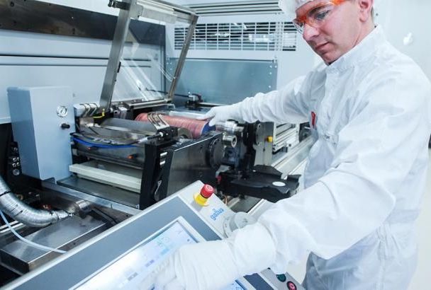
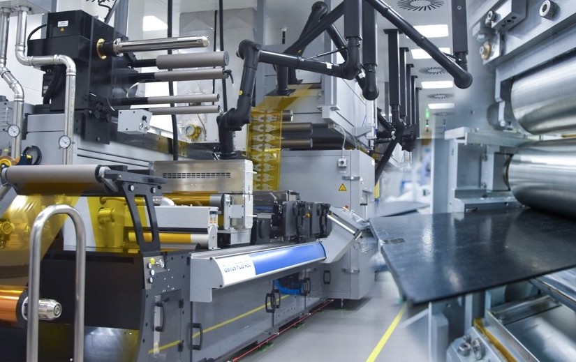
According to InnovationLab, the technology behind its ‘organic electronics’ reduces the steps behind production from nine down to just two. As such, the process is less time, cost and material intensive. The company also says 3D printing opens up a broader material palette than traditional PCB production, including flexible, biodegradable substrates, making it an ideal basis for creating novel wearables.
Elsewhere, through itsLab-2-fab服务,InnovationLab提供了帮助来自消费者,汽车,医疗保健行业等的客户,将设计中的3D印刷电子想法从设计中带入生产。该公司由公司的支持Tech-2-Market咨询套餐及其基础设施计划,其中以统一的价格雇用其在莱茵奈卡地区的设施。
While the company has traditionally acted as a facilitator of 3D printing innovation, it has itself now reached out to the SmartEEs2 consortium, to ramp up its PCB R&D, by working with partners such as theCPI,VTT Technical Research Centre of Finland,tno,Fraunhofer FEP,有机电子萨克森,eurecatandCENTI.
欧盟资助的电子创新
Over the last two years, the SmartEEs2 program has sought to help European businesses accelerate their testing, experimentation and production of flexible electronic devices. Made up of 14 partners and coordinated by France’sCEA, the project has involved inviting test proposals from qualifying businesses, with those chosen being awarded support and invited to join its pan-EU research network.
Thus far, operating as one of theEU’s Digital Innovation Hubs这项800万欧元的倡议致力于帮助公司数字化,并增强开发新型电子设备的欧洲公司的竞争力。由于该项目将于今年晚些时候结束,因此总共针对44项申请实验,据报道,该实验产生了InnovationLab和Isra的PCB 3D打印突破。
Compared to traditional PCB production processes, InnovationLab’s is said to run at a lower temperature of around 150ºC, thus making it more energy efficient. The multilayer metal and dielectric printing method also involves depositing material onto a substrate that’s fifteen times thinner, enabling users to reduce their material consumption and waste.
到目前为止,利用这项技术,该公司设法通过印刷天线创建了低功率温度传感器,NFC通信接口和紧凑的太阳能电池。随着设备在测试方面达到了目标功能,他们的开发人员现在说,其背后的过程有可能实现可持续的PCB生产和进一步的混合电子研发。
3D printing in Flexible Hybrid Electronics
Although 3D printed PCBs haven’t disrupted the traditional electronics market just yet, the technology continues to be the subject of intense research. As recently as March 2022,NextFlex向电子产品3D打印研发投入了1700万美元, with beneficiaries likeGE ResearchandLockheed Martin现在使用的资金开发3 d印刷广播frequency (RF) and hypersonic flight-related parts.
In more commercial applications,纳米尺寸’s DragonFly IV 3D printercontinues to offer users the ability to create highly-complex PCBs in a one-step process. That said, the system hasn’t really achieved widespread adoption, and while the firm’s revenue rose from $811,000 to $10.4 million between Q2 2021 and 2022, this was largely due to a string of acquisitions it finalized over the last year.
今年早些时候,nScrypt’sresearch armSciperio还宣布,它已经迈出了潜在的重要一步Factory in a Tool electronics 3D printingsystem. Sciperio patented an电子3D打印个性化治疗设备, capable of sending patient data to a video game for therapeutic training purposes.
要了解最新的3D印刷新闻,请不要忘记订阅3D打印行业newsletter或跟随我们Twitter或喜欢我们的页面Facebook.
For a deeper dive into additive manufacturing, you can now subscribe to ourYouTube频道,包括讨论,汇报和3D打印进程的镜头。
Are you looking for a job in the additive manufacturing industry? Visit3D Printing Jobsfor a selection of roles in the industry.
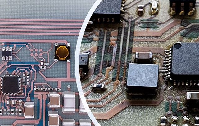
Featured image shows an InnovationLab 3D printed PCB. Image via InnovationLab.