
Since its proprietary technology launched back in 2014, industrial 3D printer OEMNano Dimension在加上生产的电子产品(AME)的世界中为自己建立了一个名称。
With ongoing refinements to its flagship蜻蜓LDM®3D打印机,该公司现在正在将其高性能电子设备(HI-PEDS™)的3D打印翻倍,该区域可以看到它取得重大成功in recent years. The Hi-PEDs™ targeted by the company often cannot be produced using traditional printed circuit board (PCB) manufacturing processes.
Yoav Stern, CEO of Nano Dimension, states, “We’re the 3D printing company for customers who need to stay on the cutting edge of electronics design. You’re creating the latest innovations in hardware development and electronic circuits. You need an additive manufacturing solution that allows you to go where no one has gone before in electronics design — and to get there faster and easier than ever before.”
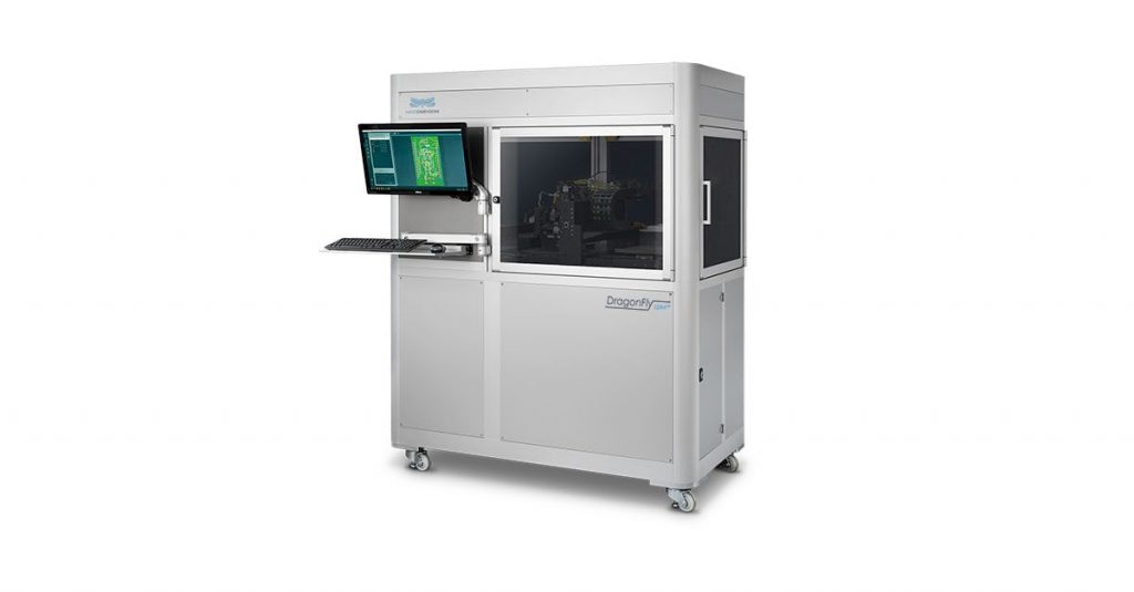
The DragonFly LDM
蜻蜓LDM®是南背后的驱动力o Dimension’s AME capabilities, combining freeform geometrics with embedded 3D electronics. Equipped with two individual printheads, the system can simultaneously deposit a conductive silver nano-ink and a dielectric photopolymer ink. The former comprises the bulk of a printed circuit’s connections, while the latter serves to provide mechanical support, thermal resistance, and electrical insulation for the surrounding structure.
Well-suited for rapid prototyping purposes, the system is safe for use in both an office and laboratory environment. Starting with a Gerber or CAD file, the user can produce customHI-PEDS™,例如复杂的多层电路with a couple of clicks. The system’s AME technology allows for many embedded electronic components, including capacitors, antennas, coils, and converters, to name a few. As an aside, the ability to install electronics in non-conventional cubic packages is also possible, whereby they are separate from the rest of the circuit boards.
斯特恩补充说:“纳米尺寸弥合了PCB和半导体集成电路之间的差距。单击按钮时的革命 - 从CAD到数小时的功能性和高性能AME设备,仅以耗资易于材料为代价。”

AME 3D printing for the ISS
Although the AME process has its uses in many industries, from medical to automotive, one project completed in collaboration with communications technology firm Harris Corporation (nowL3HARRIS) stands out. The partners worked to 3D print a radio frequency (RF) circuit for transmitting data to and from the ISS. RF circuits’ traditional production is usually a very tedious trial and error process, with numerous design iterations.
L3Harris的高级科学家Arthur Paolella博士说:“ 3D打印的应用是广泛的,几乎触及了研究,设计和制造的各个方面。该项目的主要目标是进行一个实验,该实验由添加剂制造制造的集成通信电路组成,并在太空环境中分析了这些材料的RF属性。据我们所知,这将是分析太空中这种设备的第一种系统方法。”
Having employed Nano Dimension’s AME technology, the partners 3D printed a 101 x 38 x 3mm circuit in around 10 hours. After testing the 3D printed RF circuit against a conventionally manufactured counterpart, L3Harris determined the two had very similar transmission performances. The time and cost differences were really where 3D printing shined as Nano Dimension’s RF circuit allowed for several design iterations in a much shorter space of time, ultimately resulting in reduced costs and a faster time to market.

Subscribe to the3D打印行业通讯有关增材制造中的最新消息。您也可以通过关注我们来保持联系Twitter并喜欢我们Facebook。
寻找添加剂制造业的职业?访问3D Printing Jobsfor a selection of roles in the industry.
特色图显示了Nano Dimension的AME Technology 3D打印PCB。通过纳米尺寸的照片。